Optoelectronics laboratory
[Japanese]
 Professor
Kazumasa HIRAMATSU
hiramatu@elec.mie-u.ac.jp
Associate Prof.
Hideto MIYAKE
miyake@elec.mie-u.ac.jp
Associate Prof.
Atsushi MOTOGAITO
motogaito@elec.mie-u.ac.jp
Tech. Staff
Naoaki UMEDA
umeda@elec.mie-u.ac.jp
Optoelectronics laboratory Home Page
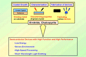
Recently, the development of semiconductor industry is remarkable. Semiconductor devices are used in whole electrical system such as electrical appliances, information processing, communications and so on. Now, Si and GaAs are mainly used. In the 21st century, semiconductor devices are required for high function and high performance. So the appearance of new devices, such as low-energy, severe environment, high-speed processing, short wavelength light emitting and so on, is waited.
In optoelectronics laboratory, we study crystal growth, characterization and application for new devices of III-nitride semiconductors (GaN, AlN, InN and AlInGaN) and chalcopyrite semiconductors (CuGaS2, AgGaSe2, etc.), which are expected for short wavelength light emitting devices, severe environment electronic devices and high efficiency solar cells. The main themes of our research are as follows.
1. Crystal growth and Characterization of III-Nitride Semiconductors
We study crystal growth and characterization of III-nitride semiconductors (AlN, GaN, InN and AlInGaN).
a) Metalorganic vapor phase epitaxy (MOVPE)
b) Hydride vapor phase epitaxy (HVPE)
c) Characterization of optical and electrical properties
2. Study of III-Nitride Semiconductors Process
We study dry etching of III-nitride semiconductors and fabrication of nano structures.
a) Reactive ion etching (RIE) mechanism
b) Fabrication of nano structures and device application
3. Application of III-Nitride Semiconductors to Optoelectronic Devices
We study fabrication and characterization of optoelectronic devices.
a) Characterization of ultraviolet photodiode
b) Fabrication and electrical characterization of Schottky barrier diode
4. Chalcopyrite semiconductors
We study crystal growth and characterization of chalcopyrite semiconductors, especially Cu-III-VI2 or Ag-III-VI2 (CuGaS2, AgGaSe2, etc.).
a) Bulk crystal growth
b) Epitaxial growth
c) Characterization of optical and electrical properties
www-admin@elec.mie-u.ac.jp
 Professor
Kazumasa HIRAMATSU